
Previous week we observed a teardown of Huawei’s Mate 40 Pro by Chinese tech web site Aio Technology and now we have a disassembly for the flashier Mate 40 RS which exposed a proprietary HiSilicon storage chip underneath.
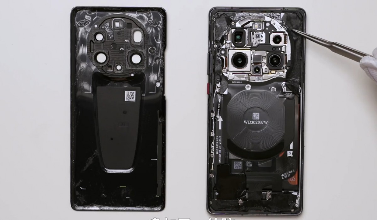
The teardown starts predictably by heating up the again of the device and working with a suction cup to pry it open up. Aside from the exclusive octagon-formed rear structure, the Mate 40 RS is virtually similar in structure to the Mate 40 Pro on the inside.
We have the five digicam modules together with the IR temperature sensor along with the NFC and wireless charging coils, 4,400 mAh battery and charging module. Disconnecting various connection cables lets you take away the motherboard and digital camera modules.
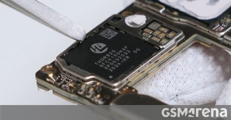
This is exactly where the appealing little bit is, we can evidently see the memory chip bears HiSilicon branding which is evidence that Huawei is developing in-house memory chips. There’s not much info out there about this precise memory storage.
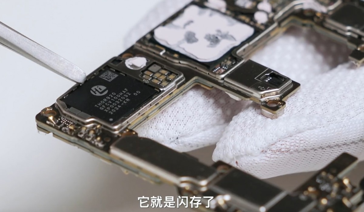
In accordance to reviews from Chinese tech bloggers, the Mate 40 Pro+ and Mate 40 RS are the first devices to use Huawei’s self-created SFS 1. flash memory which exams pretty much twice as rapidly as UFS 3.1 storage in study and generate speeds.
For every the illustration supplied, Huawei’s SFS 1. storage manages sequential publish speed at 1,280MB/s and random generate speeds of 548MB/s which are notably a lot quicker than UFS 3.1 storage which hoovers all around 700MB/s sequential produce and 200-300MB/s random compose speeds.
However, there is no official assertion from Huawei on the SFS common so just take all this facts with warning.
Source (in Chinese) | Through
Some parts of this article are sourced from:
gsmarena.com
 New Chrome Zero-Day Under Active Attacks – Update Your Browser